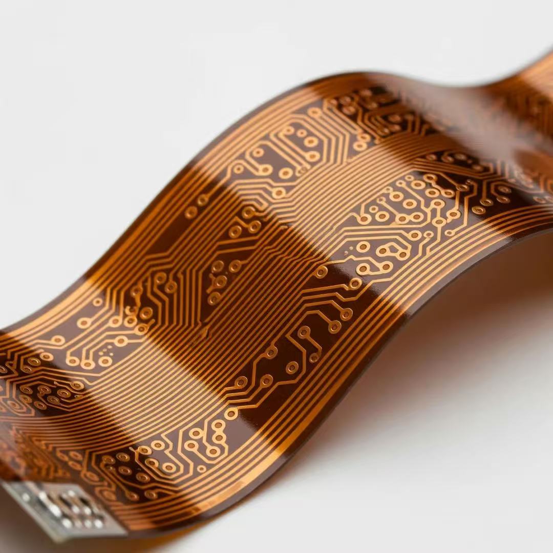
Flexible Printed Circuit is a printed circuit board (PCB) that uses a photolithography pattern transfer and etching process to create a conductive circuit pattern on a flexible substrate.
Double-sided and multi-layer PCBs use metallized vias to provide electrical connections between the surface and inner layers. The circuit pattern is protected and
insulated by a PI and adhesive layer.
These boards feature high wiring density, light weight, and thin thickness. They are primarily used in mobile phones, laptops, PDAs, digital cameras, and LCMs.

1. Advantages of FPC PCB
Flexible printed circuits (FPCs) are printed circuits made from a flexible insulating substrate. They offer many advantages over rigid printed circuits:
They can be bent, rolled, and folded freely, arranged to suit spatial layout requirements, and moved and extended in three dimensions, achieving integrated component assembly
and wiring connections.
FPCs can significantly reduce the size and weight of electronic products, meeting the trend toward higher density, miniaturization, and higher reliability.
Therefore, FPCs are widely used in aerospace, military, mobile communications, laptops, computer peripherals, PDAs, digital cameras, and other fields.
FPCs also offer excellent heat dissipation, solderability, ease of assembly, and low overall cost.
The rigid-flexible design also compensates for the limited component load capacity of flexible substrates.
2. Disadvantages of FPC PCBs
High initial cost:
Because flexible PCBs are designed and manufactured for specialized applications, the initial circuit design, wiring, and photolithography costs are high.
Unless there's a specific need for flexible PCBs, they're generally not recommended for small-scale applications.
Difficulty in modifying and repairing flexible PCBs:
Once manufactured, any changes must be made from the original base design or the pre-programmed photolithography program, making them difficult to modify.
The surface is covered with a protective film that must be removed before repair and restored afterward, making it a complex task.
Size limitations:
Before flexible PCBs became common, they were typically manufactured using a batch process. Due to the size limitations of production equipment,
they couldn't be made very long or wide.
Susceptibility to damage due to improper handling:
Improper handling by assembly personnel can easily damage the flexible circuits, and soldering and rework require trained personnel.
3. How to Calculate the Bend Radius of an FPC PCB
When an FPC is bent, the stresses on either side of its centerline differ. The inner side of the curved surface experiences compression, while the outer side experiences tension.
The magnitude of the stress depends on the thickness and bend radius of the FPC. Excessive stress can cause delamination, copper foil breakage, and other issues.
Therefore, during design, the FPC's laminate structure should be carefully arranged to ensure symmetry between the two ends of the curved surface's centerline.
The minimum bend radius should also be calculated based on the specific application.
Introduction to Calculating the Bend Radius of an FPC:
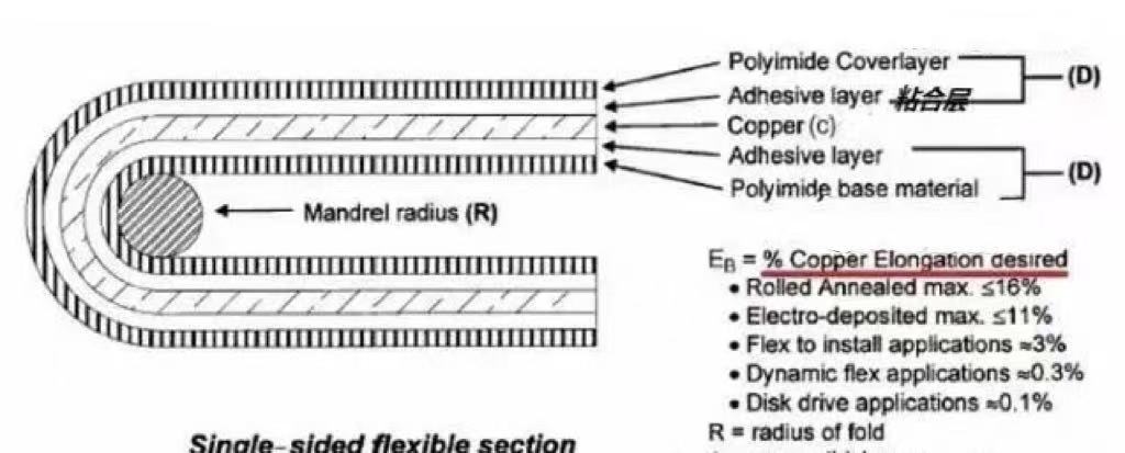
Case 1: The minimum bending of a single-sided flexible circuit board is shown in the figure below:

The minimum bend radius can be calculated using the following formula: R = (c/2) [(100 - Eb) / Eb] - D, where: R = minimum bend radius (µm), c = copper thickness (µm),
D = cover film thickness (µm), and EB = allowable copper deformation (measured as a percentage). Different types of copper have different copper deformation limits.
A. The maximum copper deformation limit for rolled copper is ≤16%.
B. The maximum copper deformation limit for electrolytic copper is ≤11%.
Furthermore, the maximum copper deformation limit for the same material varies depending on the application. For one-time bending applications,
use the critical breaking limit (16% for rolled copper). For curved installation designs, use the minimum deformation value specified in IPC-MF-150 (10% for rolled copper).
For dynamic flex applications, use a 0.3% copper deformation limit. For magnetic head applications, use a 0.1% copper deformation limit.
By setting the allowable copper deformation limit, the minimum bend radius can be calculated. Dynamic flexibility: This type of copper foil is used to
achieve functions through deformation. For example, the phosphor copper shrapnel in the IC card holder is the part that contacts the chip after the IC card is inserted.
The shrapnel continuously deforms during the insertion process. This application scenario is flexible and dynamic.
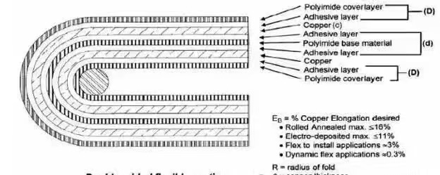
Case 2: The minimum bending of a double-sided flexible circuit board is shown in the figure below:

R = minimum bend radius (µm), c = copper thickness (µm), D = cover film thickness (µm), EB = copper deformation (percentage).
EB is the same as above.
d = interlayer dielectric thickness (µm).
Flexible PCB Minimum Bending Radius and Flexural Strength! [& w) ]# J7 U* T& J3 L
Type Minimum Bending Radius:
1.Single-sided board: 3-6 times the conductor thickness4 [1 Z- C2 n9 g
2. Double-sided board: 6-10 times the conductor thickness4 c) q* ~( e5 x
3. Multi-layer flexible board: 10-15 times the conductor thickness. p Y, E+ M9 Z/ H
4. Dynamic single-sided board: 20-40 times the conductor thickness
As electronic devices become increasingly thinner and more flexible, Flexible Printed Circuit (FPC) technology is developing at an unprecedented rate.
FPC PCB has become the core component connecting modern electronic devices and is reshaping the design concept and manufacturing methods of electronic products.