A Trustworthy PCB and Electronic Manufacturing Enterprise! Contact Us

Your smartphone, laptop, and even your car rely on printed circuit boards (PCBs). What if the PCB inside your phone contained toxic chemicals like lead and mercury? Thanks to RoHS PCBs,
it doesn’t have to. In this blog, we’ll explore how RoHS PCBs are reshaping electronics—for a safer planet and smarter business.
RoHS is a mandatory standard established by EU legislation, known as the "Restriction of Hazardous Substances in Electrical and Electronic Equipment." RoHS 1.0, the old Directive 2002/95/EC,
came into effect on July 1, 2006. Subsequently, RoHS 2.0, the new Directive 2011/65/EU, came into effect on July 21, 2011, and officially replaced the old directive on January 3, 2013,
expanding the scope of control and adding new restricted substances.

The scope of ROHS-regulated products includes not only PCBs but also all components, raw materials, and packaging used in production, impacting the entire production chain.
Regulated Product Categories (Electrical and electronic products with a voltage below AC 1000V or DC 1500V):
1. Large household appliances
2. Small household appliances
3. IT and telecommunications equipment
4. Consumer equipment
5. Lighting equipment
6. Electrical and electronic tools
7. Toys, leisure, and sports equipment
8. Medical devices
9. Monitoring and control instruments, including industrial monitoring and control instruments
10. Automatic dispensers
11. Other EEE not covered by any of the above categories
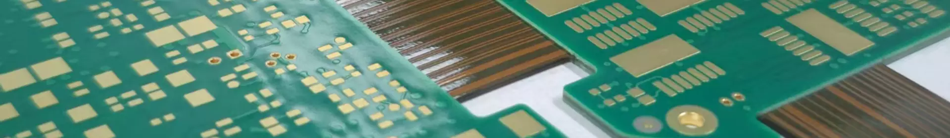
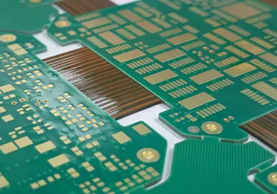
Close-up of a ROHS-compliant PCB with lead-free solder joints and halogen-free solder mask, meeting EU hazardous substance restrictions (ROHS Directive). Ideal for electric vehicle
electronics (EV PCB) and industrial control systems, manufactured with sustainable processes (Eco-Friendly PCB) and recyclable materials (Green Electronics)."
The EU RoHS Directive requires PCB manufacturers to ensure that their electrical and electronic products do not contain specified hazardous substances exceeding specified limits.
Manufacturers must conduct product testing, prepare technical documentation, provide a Declaration of Conformity, and affix the CE mark to the product to demonstrate compliance.
Furthermore, companies need to monitor their supply chains to ensure that all components and materials comply with RoHS requirements and conduct product recalls when necessary.
Below are RoHS's requirements for hazardous chemicals:

RoHS (Restriction of Hazardous Substances) restricts 10 hazardous substances in electronic products, with additional substances still under review.
The implementation of this regulation has also significantly changed the PCB manufacturing industry, driving innovations in lead-free soldering, halogen-free materials,
and environmentally friendly manufacturing.
As carriers for various components, the reliability of PCBs is crucial. PCB components primarily include substrate material, solder resist, marking, and surface treatment.
Control over the solder resist, marking, and surface treatment primarily involves controlling the composition of the materials. Surface treatments can include lead-free tin spraying,
immersion gold, or OSP.
1.Innovation in Material Systems
The PCB manufacturing process now utilizes halogen-free substrate materials certified by IATF 16949, demonstrating exceptional resistance to electrolyte corrosion - a critical advancement
for new energy vehicle BMS PCB. Through strategic partnerships with material suppliers, the industry is developing biodegradable PCB substrates incorporating plant fibers and decomposable resins.
These eco-friendly PCB materials can rapidly decompose in natural environments, significantly reducing e-waste generation.
For solder mask technology, water-based inks have achieved three breakthroughs:
Organic solvent content reduced below 5% VOCs emissions ≤15g/m² (EU limit: 100g/L)
Heavy metal purification ensures hexavalent chromium-free PCBs
Passes 288°C/10-second thermal shock tests, complying with IPC-SM-840C Class III standards for high-reliability applications
2. Revolutionized Production Processes
To address heavy metal pollution from copper etching wastewater, the PCB manufacturing industry has implemented dual resource recovery solutions:
Ion exchange membranes recover 90% copper ions for reuse in plating processes
Catalytic oxidation converts residual hydrogen to nitrogen (emission concentration<15mg/L)
The closed-loop water treatment system achieves zero wastewater discharge, aligning with the EU's New Battery Regulation requirements for sustainable supply chains
In manufacturing technology, advanced PCB production combines:
Step-and-repeat exposure technology
Intelligent panelization algorithms
Enabling mass production of 600mm×600mm large-format PCBs with 37% improved material utilization
3. Comprehensive Compliance Certification System
The PCB manufacturing process implements a three-tier quality control and traceability system:
Raw Material Screening: XRF rapid testing for cadmium, lead, and mercury (detection limit: 5ppm)
Process Monitoring: HPLC analysis of PBBs/PBDEs flame retardants (accuracy: 0.01%)
Final Product Inspection: Micro-CT scanning and AI-based defect detection, maintaining a yield rate of 99.95%+
Industry practice has demonstrated that ROHS compliance, far from being a cost burden, serves as a pivotal driver for technological evolution.
The deep integration of molecular-level optimization in inorganic solder materials with revolutionary nano-ceramic substrate innovations has positioned sustainable manufacturing as
the defining competitive dimension in high-end PCB production. This synergy between eco-conscious regulation and cutting-edge material science is reshaping industry standards,
proving that environmental responsibility and technological progress can advance hand in hand to create next-generation electronic solutions.