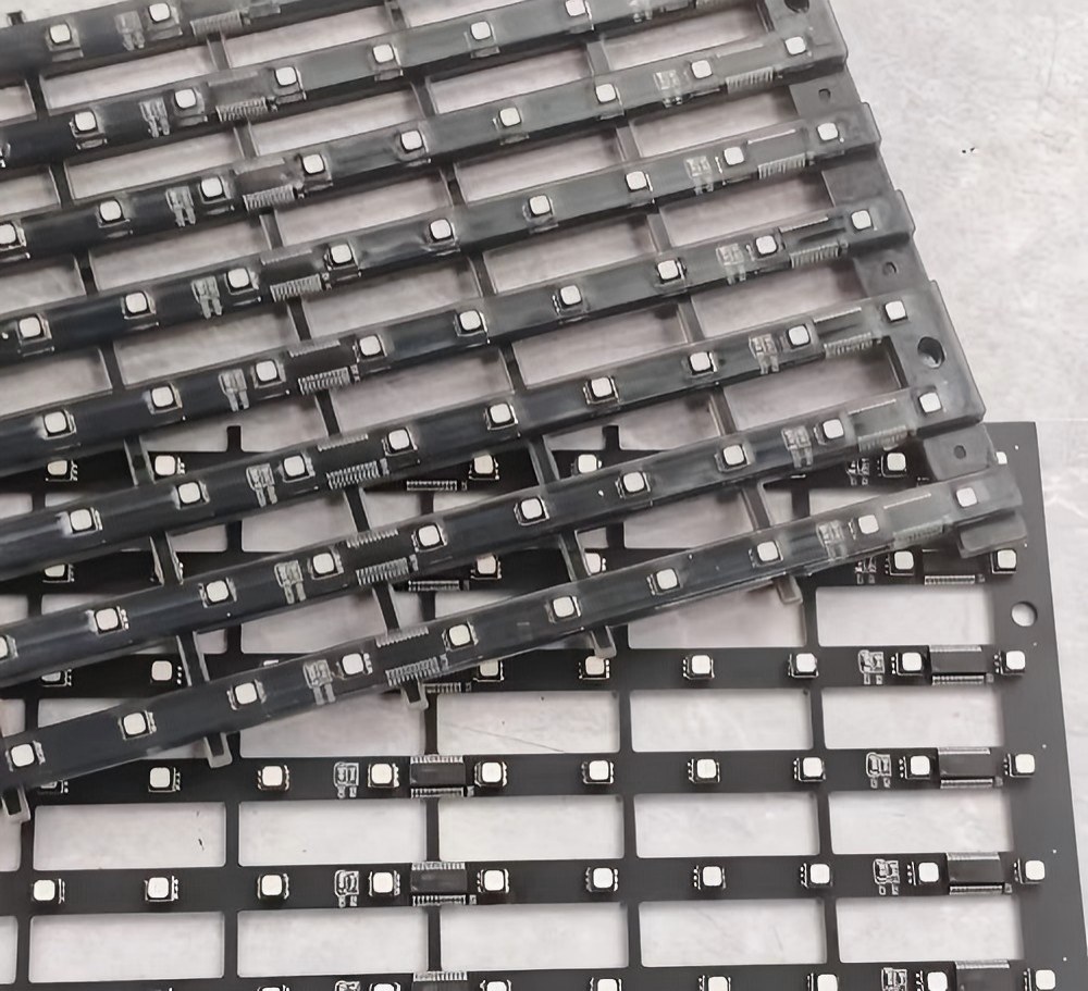
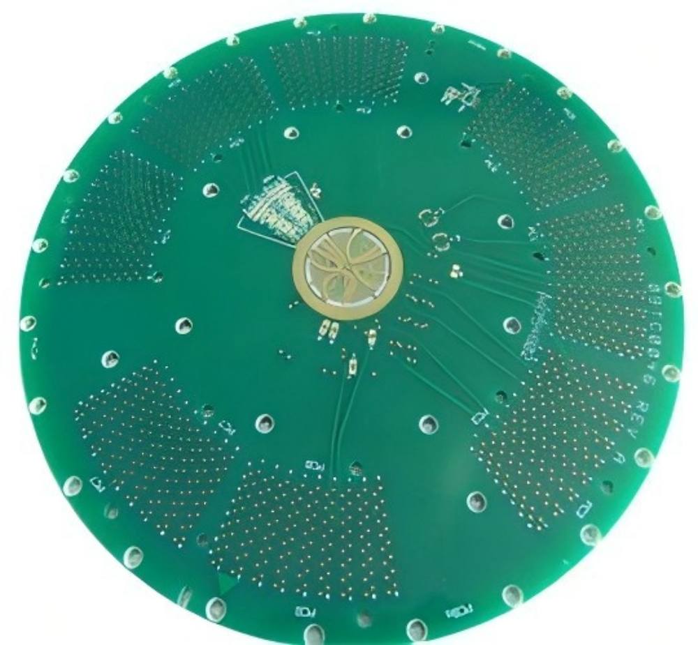
In today's rapidly evolving electronics industry, flexible printed circuits (Flex PCBs) have become indispensable components in products ranging from medical wearables to automotive control systems. However, as devices continue to shrink and operate in increasingly harsh environments, a critical question arises: How can we effectively protect these delicate, flexible circuits from mechanical stress, moisture, and chemical corrosion? The solution lies in the PCB overmolding process. By encapsulating flexible circuit boards, manufacturers can significantly enhance durability and reliability while enabling more compact designs and extended product lifespans.

What is PCB Overmolding?
1. Core Concept: A PCB board with soldered components is placed into a mold as a preform. After closing the mold, liquid silicone rubber is injected—the silicone cures under heat, forming a protective elastomer layer around the PCB and components.
2. Final Product Characteristics:
a. Internal Core: The PCB responsible for circuit functionality and its electronic components.
b. External Protective Layer: Soft, dense, insulating, and weather-resistant silicone rubber.
c. Integrated Assembly: Forms a highly integrated, rugged, and durable “three-proof” electronic module.
Key Advantages of PCB Overmolding:
1. Enhanced Mechanical Protection: The encapsulation layer effectively prevents physical damage from vibration, impact, and compression, making it suitable for high-stress operating environments.
2. Improved Environmental Tolerance: Offers superior waterproofing, dustproofing, and chemical corrosion resistance, particularly suited for outdoor and industrial settings.
3. Extended Lifespan: Significantly prolongs product service life in harsh conditions by sealing and protecting flexible circuits.
4. Enhanced Aesthetics and User Experience: Improves tactile feel and cable appearance, ideal for consumer electronics requiring human-machine interaction.

Primary Application Areas:
The core purpose of PCB silicone encapsulation is protection and sealing, primarily applied in harsh environments or high-reliability scenarios.
1. Automotive Electronics:
a. Engine Control Units (ECUs), Sensors: High-temperature resistance, oil resistance, vibration resistance.
b. In-vehicle Chargers, Control Modules: Moisture resistance, dust resistance.
c. Battery Management Systems (BMS) for New Energy Vehicles: High insulation, thermal conductivity.
2. Consumer Electronics & Outdoor Equipment:
a. Drone Flight Controllers & ESCs: Waterproofing, moisture resistance, corrosion resistance.
b. Internal Core Boards for Action Cameras/Outdoor Surveillance Cameras: Waterproofing, shock resistance.
c. Smart Wearables: Achieves swimming-grade or diving-grade waterproofing.
3. Industrial Control & Automation:
a. Industrial Sensors: IP67/IP68 protection rating, resistant to acids, alkalis, dust, etc.
b. PLC Modules: Stable operation in harsh industrial environments.
c. Outdoor Communication Equipment: Moisture-proof, salt-fog resistant.
4. Medical Devices:
a. Implantable or In-Body Devices: Utilize biocompatible silicone for electrical insulation and biological protection.
b. Handheld Medical Instruments: Resistant to sterilization and liquid ingress.
5. LED Lighting:
a. Outdoor LED Drivers: Fully sealed for waterproofing, moisture resistance, and UV protection.
b. LED Strip Lights: Encapsulate entire PCB and LEDs for flexible lighting and comprehensive protection.
Process Flow (Using Liquid Silicone Rubber LSR as Example):
1. PCB Pre-Treatment (Critical):
a. Soldering and Testing: All components must be fully soldered and undergo comprehensive functional testing, as repairs are nearly impossible after encapsulation.
b. Cleaning: Thoroughly remove flux residues, dust, and ionic contaminants from the PCB surface using ultrasonic cleaning or similar methods. Any contaminants severely impact adhesion and electrical performance.
c. Spot Adhesive/Potting: Pre-apply localized adhesive to secure large, heavy, or fragile components (e.g., large inductors, electrolytic capacitors) to withstand high-pressure impacts during injection.
d. Primer Application: Precisely apply specialized electronic-grade primer to PCB areas requiring silicone bonding (typically component-free zones like board edges or around connectors) to enhance adhesion.
2. Mold and Injection:
a. Mold Design: Extremely precise. Requires accurate positioning mechanisms to secure the PCB, preventing warping or displacement. Injection ports and runner designs must ensure smooth, uniform silicone filling to avoid excessive pressure shocks that could damage precision components.
b. Vacuum Injection: For complex, component-dense PCBs, vacuum injection is typically required. This evacuates air from the mold cavity, completely preventing bubbles from becoming trapped beneath components or between densely packed pins.
3. Vulcanization Curing:
a. The mold is maintained at the appropriate temperature to cure the LSR. Temperature and time must be precisely controlled to avoid thermal damage to heat-sensitive components.
4. Post-Processing and Inspection:
a. Deburring: Removing any burrs generated.
b. Full Functional Testing: Re-testing the encapsulated module to ensure the PCB remains undamaged during injection molding.
c. Environmental Reliability Testing: Conducting sampling tests for temperature cycling, humidity, vibration, etc., to validate the encapsulation's reliability and protection rating.

Advantages and Disadvantages of PCB Overmolding:
Advantages:
a. Unparalleled Protection: Provides comprehensive waterproofing, moisture resistance, dustproofing, corrosion resistance, and shock protection, achieving IP68 ratings.
b. Superior Electrical Performance: High insulation strength prevents short circuits.
c. Excellent Thermal Conductivity: Silicone effectively dissipates heat generated by components.
d. Structural reinforcement: Silicone acts as a shock absorber and buffer, protecting the PCB from damage in vibrating environments.
e. Miniaturization and lightweight: Replaces traditional metal casing + potting compound solutions for a more compact structure.
Disadvantages:
a. High cost: Expensive molding costs and complex manufacturing processes.
b. Virtually non-repairable.
c. Strict requirements for PCB design and component selection.
d. Significant process development complexity and high yield control challenges.
Summary:
PCB overmolding represents a high-end electronic packaging technology pursued for ultimate reliability and environmental adaptability. It is exceptionally well-suited for mass-produced electronic products demanding stringent durability requirements. To ensure success, structural engineers, electronics engineers, and silicone mold manufacturers must collaborate on the design from the project's inception.