A Trustworthy PCB and Electronic Manufacturing Enterprise! Contact Us

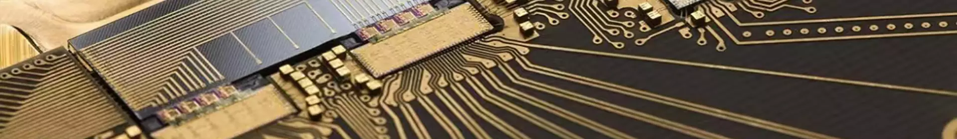
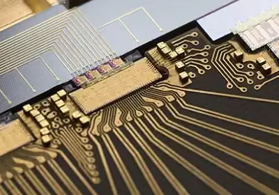
Printed circuit board (PCB) manufacturing is essentially the process of forming a predetermined conductive pattern on a copper layer above an insulating substrate
through the selective removal (subtractive process) and selective addition (additive process) of material. Among the many chemicals involved in achieving this goal,
the function and performance of one class of materials directly determine the precision, performance, and reliability of the final product: etching fluid.

The function of an etching solution is to remove all copper foil not protected by a resist layer (such as photoresist or metal plating) through a chemical reaction
after the pattern transfer process. This is a typical "subtractive" process, the goal of which is to preserve the protected circuit pattern as a physical circuit.
This is what we discussed in the previous article: etching aims to remove copper, but neither too much nor too little.
The etch factor (Etching Factor) is the primary metric for evaluating etching quality. It is defined as the ratio of etch depth to lateral etch width (undercut).
Due to the isotropic nature of the chemical reaction, the etching solution will erode the circuit sidewalls while reacting vertically downward. Excessive undercutting can lead to
undercutting of the circuit, making the final line width smaller than the designed value, directly affecting the circuit's characteristic impedance and current carrying capacity.
Therefore, achieving a high etch factor—that is, achieving steeper circuit sidewalls—is the core goal of etching solution technology.
Currently, the mainstream etching processes are mainly divided into the following three categories:

1. Acid Etching
This is the most mainstream and widely used etching technology in the PCB industry, particularly suitable for the fabrication of fine circuits.
Working Principle: Etching Reaction:
Cu + CuCl₂ → 2CuCl (converts metallic copper to cuprous chloride).
Regeneration Reaction:
2CuCl₂ + 2HCl + H₂O₂ → 2CuCl₂ + 2H₂O (an oxidant reoxidizes cuprous chloride to etching-capable cupric chloride, regenerating hydrochloric acid).
Main components of the etching solution:
CuCl₂ (copper chloride), HCl (hydrochloric acid), NaCl (sodium chloride) or NH₄Cl (ammonium chloride), an oxidant (such as H₂O₂, sodium chlorate), and additives.
The core chemical reaction is a reversible process: through a continuous regeneration system, the etching solution can maintain a stable etching rate and performance.
Features:
Minimal undercutting and a high etching factor: these are its greatest advantages. A high etch factor means the vertical etching rate is much faster than the lateral one,
resulting in steep circuit sidewalls and making it ideal for the production of fine circuits and high-density interconnects.
Stable etching rate: An automated control system monitors and adjusts parameters such as redox potential, specific gravity, and pH, maintaining long-term stability in the
etchant's activity and ensuring batch-to-batch consistency.
High film requirements: A dry film with strong acid resistance or a high-quality wet film is required.
2. Alkaline Etching
Working Principle:
CuCl₂, NH₃·H₂O (ammonia), and NH₄Cl (ammonium chloride) form a copperammine complex [Cu(NH₃)₄²⁺], which has the ability to etch copper.
This complex can also be regenerated by introducing air or oxygen.
Features:
Tin/lead-tin resist-friendly: This has traditionally been its main advantage. Alkaline environments do not attack metallic tin, making it suitable for use with processes
using tin as a resist (referred to as "tin etching" processes). High copper solubility: Alkaline etchants can accommodate high copper concentrations (up to 150-190 g/L)
without a significant drop in performance.
Severe side etching and low etching factor:
Alkaline etching exhibits poor anisotropy, with pronounced lateral etching, which can easily lead to a "pear-shaped" cross-section. This also results in poor linewidth control accuracy,
making it unsuitable for fine lines.
3. Persulfate Etching
This is an older process and is now less common. It is primarily used in laboratories, small-batch production, or special applications.
Working Principle:
Main components of the etching solution: ammonium persulfate [(NH₄)₂S₂O₈] or sodium persulfate (Na₂S₂O₈). Etching reaction: S₂O₈²⁻ + Cu → Cu²⁺ + 2SO₄²⁻
Features:
Chlorine-free: The solution contains no chloride ions, eliminating potential problems caused by residual chloride ions. Simple chemical composition:
Contains no strong acids or bases, making operation relatively safe.
Low etching factor: Severe undercutting occurs, resulting in poor circuit precision control.
Poor stability and short lifespan: The etching solution decomposes spontaneously, especially at high temperatures and under the influence of metallic impurities.
Its performance degrades rapidly, making it non-regenerative and requiring frequent replacement.
Issues to note during PCB etching:
Side etching can cause overhangs. Generally, the longer the printed circuit board is in the etching solution, the more severe the overhang. Side etching can severely affect the precision
of printed traces, and severe undercuts make it impossible to produce fine traces. When undercuts and overhangs are reduced, the etching coefficient increases.
A high etching coefficient indicates the ability to maintain fine traces, allowing the etched traces to approach the original dimensions.
Whether using tin-lead alloy, tin, tin-nickel alloy, or nickel electroplating etchants, excessive overhangs can cause short circuits. This is because overhangs can easily tear off,
creating an electrical disconnect between two points on the conductor.