A Trustworthy PCB and Electronic Manufacturing Enterprise! Contact Us

The electronics industry is experiencing robust growth driven by the explosive demand for AI computing power, with PCB emerging as a particularly prominent player
as a critical link in the AI supply chain.
AI servers impose stricter low-loss requirements on PCB products that carry signal channels. Related hardware equipment undergoes rapid upgrades and iterations,
and product forms differ significantly from traditional wired products. For PCBs themselves, AI and high-speed network infrastructure demand extremely high data processing
and transmission speeds. This necessitates achieving high-speed signal transmission, high-density integration, and high reliability within limited space.
Addressing complex issues like signal interference and power distribution drives PCBs toward greater complexity, higher performance, increased layer counts,
and HDI (High-Density Interconnect) development.
1. PCB—The Core Carrier of Electronic Components
PCBs not only provide electrical connections for electronic components but also handle digital and analog signal transmission, power supply,
and RF/microwave signal transmission/reception for electronic devices. Widely used in communication electronics, consumer electronics, computers, data centers,
automotive electronics, industrial control, and medical devices, they are indispensable components in modern electronic information products,
earning the title “Mother of the Electronics Industry.”

Key Role of PCBs: Electronic packaging is categorized into four tiers, analogous to building construction: wafer-level packaging is the foundation (Tier 0),
chip-level packaging forms the main structure (Tier 1), board-level packaging connects internal pipelines (Tier 2), and system assembly constitutes the entire building (Tier 3).
PCBs fall under Level 2 packaging, serving as the “interconnection bridge + support platform” for electronic components.
They secure various parts in place while establishing electrical pathways between them, enabling smooth signal transmission during electronic assembly and testing.
IC packaging substrates belong to primary packaging, serving as the chip's “dedicated bodyguard + connector.” They provide support, protection,
and thermal management for the chip while establishing the electronic pathway between the chip and the PCB. They are core materials in semiconductor packaging and testing.
2. PCB Classification
Rigid PCB: Manufactured from inflexible substrates with moderate strength and toughness, these boards offer bending resistance
and provide structural support for mounted electronic components. Rigid substrates include fiberglass cloth substrates, paper substrates, composite substrates,
ceramic substrates, metal substrates, and thermoplastic substrates. Widely used in computer and network equipment, communication devices, industrial control systems,
consumer electronics, and automotive electronics.
Flexible PCB: Printed circuit boards made from flexible insulating substrates that can be freely bent, rolled, or folded. They enable arbitrary spatial layout arrangements,
integrating component assembly and wire connections. Extensively applied in smartphones, laptops, tablets, and other portable electronic devices.
Rigid-Flex PCB: Incorporates one or more rigid zones and flexible zones on a single board. Manufactured by laminating thin flexible PCB layers to rigid PCB substrates,
it combines the structural support of rigid boards with the bending flexibility of flexible boards, meeting three-dimensional assembly requirements.
Widely used in advanced medical electronics, portable cameras, and foldable computing devices.
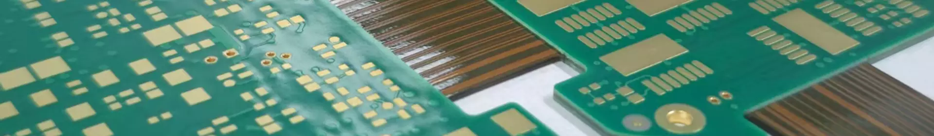
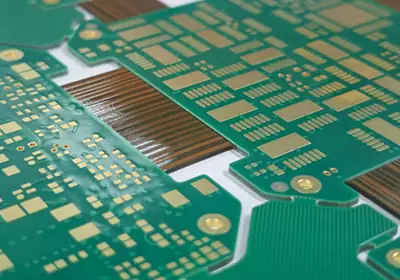
HDI PCB: Typically manufactured using the multilayer stacking method, it employs laser drilling technology for interlayer connections primarily via buried and blind vias.
This enhances routing density, improves signal output quality, and reduces product size. Applied in digital products like mobile phones, laptops,
and automotive electronics (most prevalent in mobile phones), it is now adopted in communications, networking, servers, automotive, and even aerospace products.
IC Substrates: Directly mount chips, providing electrical connections, protection, support, thermal dissipation, and assembly functions. Achieve multi-pin configurations,
reduced size, and improved electrical performance. Widely used in mobile communication products like smartphones and tablets.
High-speed communication packaging substrates are also employed in data broadband applications.
Standard PCB: Manufactured using FR4 copper-clad laminate (typically Dk > 4.0@11GHz, Df > 0.015@1GHz) to address basic electrical continuity
with lower signal integrity requirements. Widely used in communication equipment, network devices, computers/servers, consumer electronics, industrial control,
and medical applications.
High-Frequency PCB: Manufactured using high-frequency laminates (exhibiting strong Df and Dk stability, with stringent requirements for electrical performance consistency
under temperature/humidity variations and long-term aging; Df requirements typically exceed those of high-speed materials). Primarily applied in wireless communication,
automotive ADAS, and other products involving wireless signal transmission/reception.
High-Speed PCB: Manufactured using high-speed copper-clad laminates (typically Dk ≤ 4.0@1GHz, Df ≤ 0.015@1GHz). Beyond basic electrical connectivity,
they impose specific requirements on high-speed signal transmission stability and integrity. Primarily used in wired communications, network equipment, computers/servers,
and similar fields.
This article introduces the basic classifications of PCBs. In the next installment, we will explore the end-use applications of AI PCBs.