In hardware design, RF antenna design is quite demanding. Besides performance, cost must also be considered, so antenna selection requires comprehensive considerations.A common low-cost design approach is PCB-mounted antenna design.
For 2.4GHz applications, most PCB antennas fall into the following categories:
1. Planar Inverted-F Antenna Design, or PIFA
For RF, any copper foil or wire cannot be considered a simple wire; it is an equivalent circuit composed of many resistors and capacitors. When we see a short circuit,
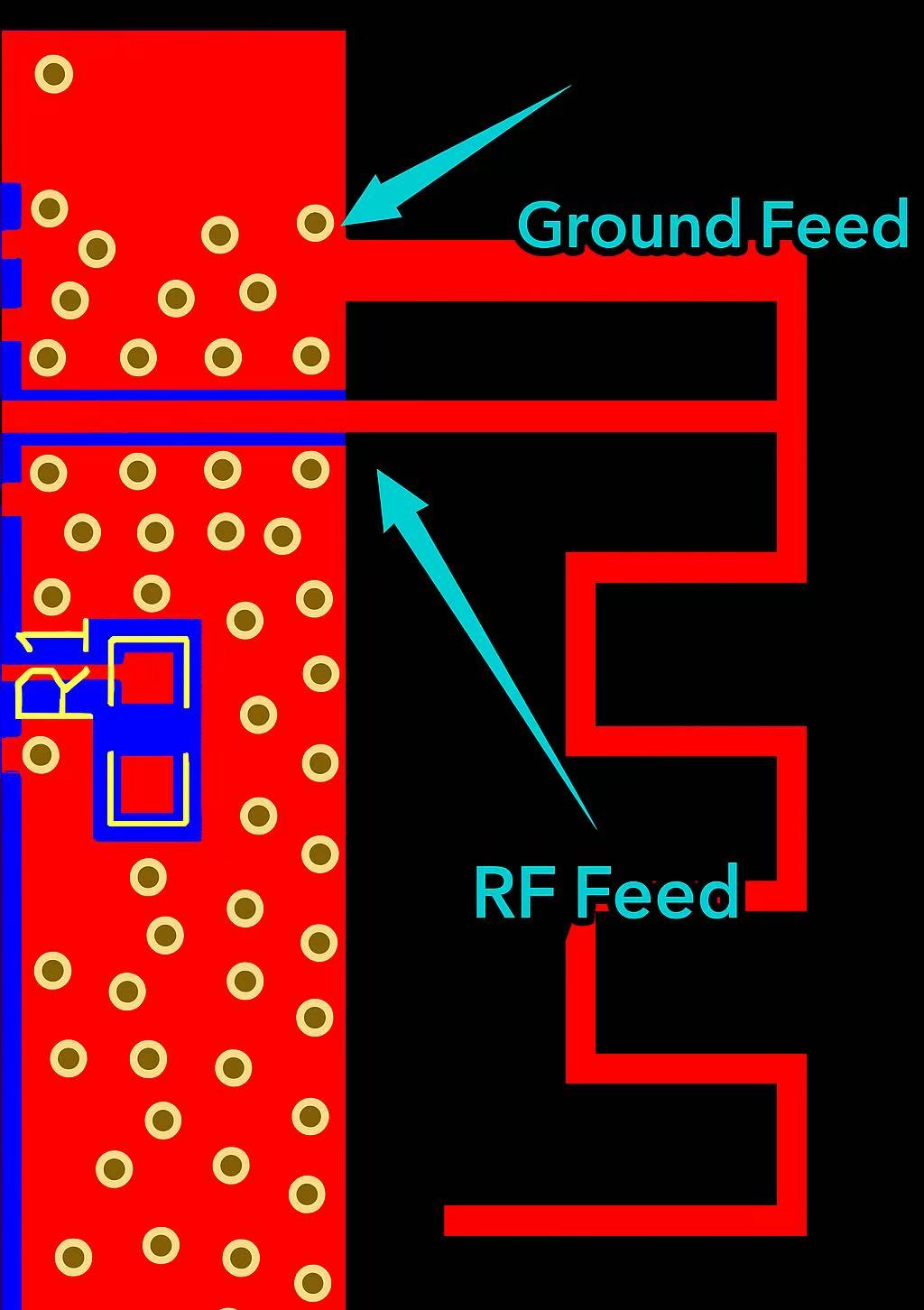
it's not a short circuit for RF. Using this approach, let's examine the key points to consider when designing an inverted-F antenna (using the following figure as an example):

a. This inverted-F antenna isn't something you can just draw casually. There's a library of wires available; simply use them and place them as required.
If space is limited, you can create your own custom antenna through simulation.
b. The impedance of the trace leading out of the RF feed point must be 50 ohms.
c. The ground feed point must be securely grounded.
d. The ground plane must have multiple ground vias, as shown in the figure above.
e. The copper foil on all layers around the antenna must be clear.
f. The antenna must be placed in a corner of the PCB board, ideally with three sides clear. As shown in the figure, the top three sides are clear.
Inverted-F Antenna Design for Bluetooth:
The antenna body of an inverted-F antenna can be linear or sheet-shaped. Using insulating materials with a high dielectric constant can also reduce the size of the Bluetooth antenna.
As a type of board-mounted antenna, the inverted-F antenna design offers low cost but increases size. It is the most common design in practical applications.
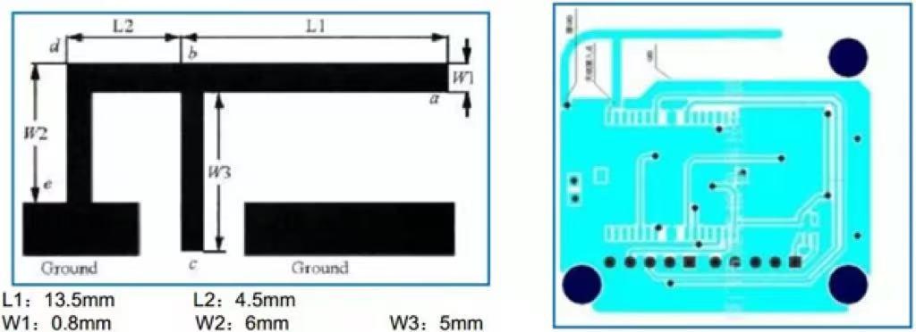
The antenna is typically placed on the top layer of the PCB, with the ground plane typically placed on the top layer near the antenna. However, the antenna must be free of ground and
surrounded by clear space. See the figure below:

2. Inverted-L-Shaped PCB Board-Mounted Antenna Design
There are many PCB board-mounted antennas on the market, primarily the types shown in the figure below.

In RF hardware development, selecting the correct PCB board-mounted antenna is only the first step in achieving optimal wireless performance. The RF antenna serves as the “signal output,”
but it is the RF PCB that acts as the “highway” transporting those signals. If the PCB is poorly designed—especially in terms of ground plane integrity and via placement—the result can be signal loss, interference, impedance mismatch, or even total communication failure.
RF PCB (Microwave RF Circuit Board) Ground Plane Design:
1. The ground plane, which serves as the mirror image return path for RF signal lines, must be complete and independently defined, with no other signal lines routed on the ground plane;
2. Unless it can be ensured that current will not form a loop on the ground plane, the ground plane should not be divided;
3. For high-density PCBs (such as those using CSP packaging), dual-layer PCBs are not recommended. Instead, four-layer RF PCBs (high-frequency pure laminates orhigh-frequency hybrid laminates) should be used for design;
4. The ground plane beneath RF signal lines should be as wide as possible. Narrow ground planes can cause parasitic parameters and increase attenuation;
5. The ground plane and the top layer ground should be connected via vias between the two layers. It is essential to ensure that RF signal lines are fully “shielded” to
enhance the product's EMC performance;
6. For the blank areas on the Top Layer and Bottom Layer, it is recommended to apply a ground plane and connect all ground areas via vias with a spacing no greater than λ/20;
7. It is also recommended to wrap the power plane with ground vias to avoid unnecessary electromagnetic radiation.
Typically, the power plane must adhere to the “20H” principle relative to the ground plane. The “20H principle” requires that the edge of the power plane be indented at least 20 times
the distance between the two planes from the edge of the ground plane (0V reference plane), where H represents the distance between the power plane and the ground plane. At 20H,
70% of magnetic flux leakage can be suppressed, effectively improving EMI performance.
1. Use as many vias as possible to connect different layers, with intervals no greater than λ/20 of the signal wavelength;
2. “Ground via accompaniment”: place as many vias as possible near signal lines to reduce via parasitic inductance;
3. Avoid RF signals crossing layers as much as possible;
4. Avoid sharing vias between pads and solder joints; keep them independent as much as possible;
5. Use ground vias to isolate interference sources from sensitive circuits;
6. For QFN-packaged devices, use as many vias as possible on the bottom pads;
Ultimately, RF PCB design and RF antenna design are inseparable. Even the most advanced antenna will underperform if the PCB layout fails to provide a clean, low-loss environment for RF signals. By integrating thoughtful ground plane strategies, optimized via placement, engineers can unlock the full potential of their RF antenna design, achieving stable impedance, reduced EMI, and consistent wireless performance across real-world conditions.