In the fast-paced world of electronics manufacturing, product design trends are moving toward smaller, lighter, and more aesthetically pleasing devices.
This shift is especially visible in industries like wearables, smart devices, LED lighting, drones, medical equipment, and automotive electronics. In many of these applications, a traditional rectangular PCB is no longer the optimal choice — instead, the Round PCB, also known as a Circular PCB, has become the go-to solution.

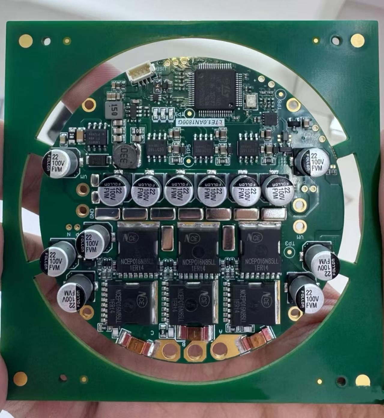
A circular PCB is essentially a printed circuit board with a circular design, rather than a standard square or rectangular layout. While this may sound like a minor design change,
it can make a huge difference in performance, space utilization, and product aesthetics.
In addition to high density, high-speed signal transmission, and excellent power management, circular PCBs offer several other advantages:
High reliability: Due to their unique design, the components and connections on through-hole PCBs undergo rigorous quality control and testing, resulting in high reliability.
Adaptability: The design of circular through-hole PCBs can be customized to meet specific application requirements, making them highly adaptable.
High anti-interference capabilities: Due to the design of their ground and power planes and optimized circuit layout, circular through-hole PCBs exhibit strong anti-interference capabilities.
Lightweight: Due to their small size and compact structure, circular through-hole PCBs are relatively lightweight, making them easy to install and use.
Cost-effectiveness: Circular through-hole PCBs can be manufactured in batches, making them highly cost-effective.
In summary, circular PCBs have unique design and excellent performance, and are suitable for various application scenarios that require high-density, high-speed signal
transmission and excellent power management. At the same time, they have the characteristics of high reliability, strong adaptability, strong anti-interference ability, light weight and high
cost-effectiveness.

1、Types of Circular PCBs
Circular PCBs come in various types. These include:
Single-Sided Circular PCBs
Double-Sided Circular PCBs
Multi-Layer Circular PCBs
Single-sided circular PCBs have a single conductive copper layer. This type of PCB is widely used in low-density designs. They feature components on one side of the board
and a conductor pattern on the other. These PCBs utilize through-hole or surface mount technology.
Double-Sided Circular PCBs have conductive layers on both sides of the board. They are widely used in applications such as wearable devices and lighting systems.
Multi-Layer Circular PCBs have more than two conductive layers. While they are the most difficult to manufacture, they are suitable for higher densities while providing more board space.
2. Designing a Circular PCB:
Creating a circular PCB layout is more than just reshaping a square board. It requires precision, the right tools, and smart planning.
Using the Right CAD Tools
Start with CAD software that supports custom shapes, such as Eagle, Altium Designer, or BaseCAD. These tools help you easily draw clean outlines, place components,
and handle curved layouts.
Drawing Precise Circular Outlines
Rather than drawing freehand, always use precise tools to create circular layouts. In Eagle, start by drawing a square, then use the Miter command.
Make sure all sides are equal to keep the board truly circular, not oval or off-center.
Planning Component Placement
Space on a circular PCB is limited, especially near the edges. Place important components such as chips and connectors closer to the center. Place smaller or less important components in the
peripheral areas. This helps with balance, soldering, and thermal stability.
Tracing Routes Smoothly
Curved designs can make routing a bit tricky. Use smooth, angled paths instead of sharp corners. Keep traces short, clean, and evenly spaced—especially on high-speed or sensitive circuits.
Defining Power and Ground Planes
Use the polygon editor in your CAD tool to shape the power and ground planes to match the board. Well-designed planes help with signal stability, thermal management, and EMI reduction.
Avoid sharp edges or damaged fillets that can cause electrical problems.
Think Manufacturing
A good design should be easy to manufacture. Leave ample space between the copper and the board edge. Adhere to standard sizes for pads, holes, and layers whenever possible.
The simpler the layout, the more reliable and cost-effective it is.
3. Round PCB Panelization and Manufacturing Challenges
Design is only the first step—manufacturing round PCBs presents its own unique challenges. Due to their shape, they cannot be machined like rectangular boards.
Interrupt Routing is a Must
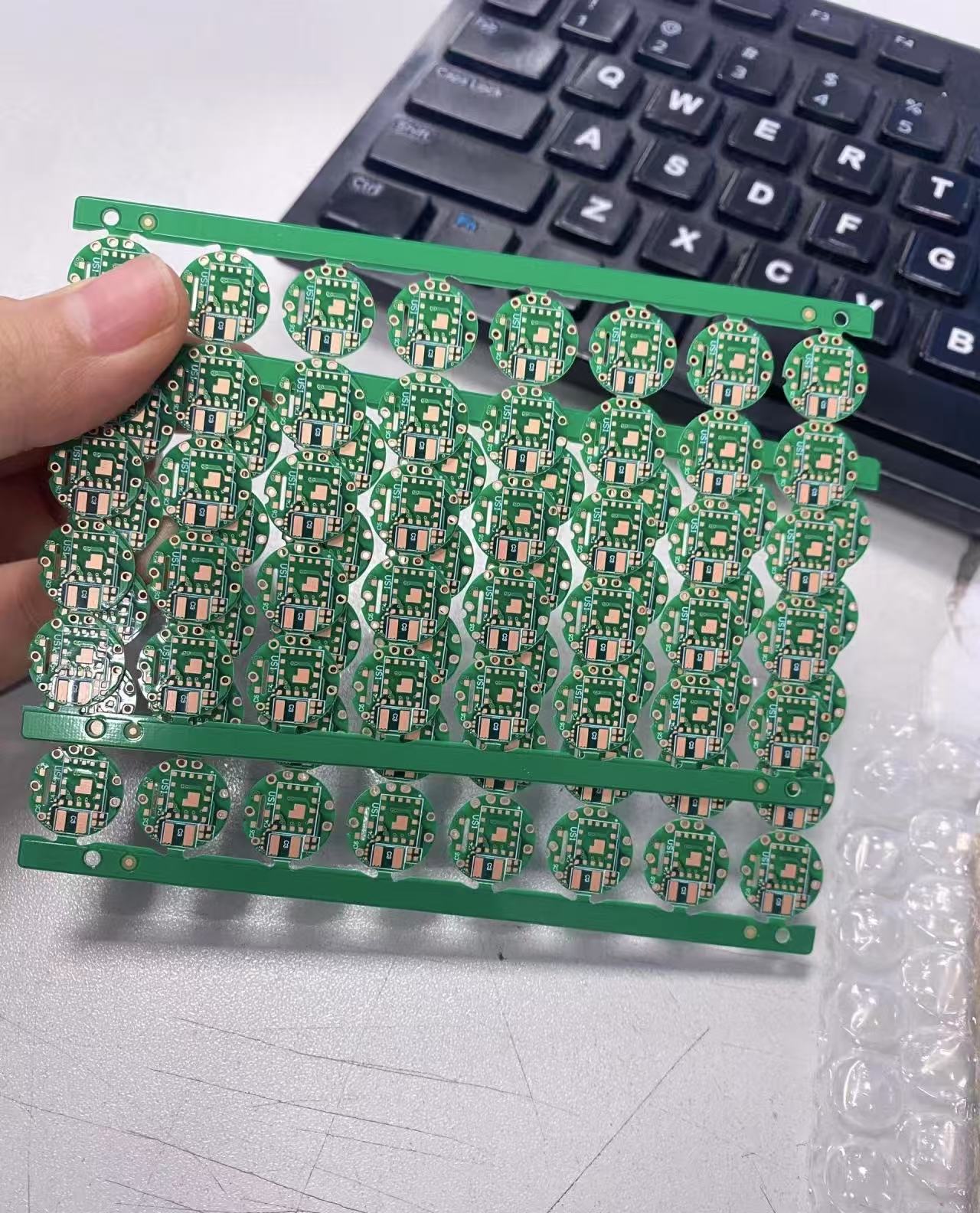
Unlike square boards, which can be separated with a straight cut, round PCBs require interrupted routing.
This method uses small protrusions to hold each board in place during production, which are then broken or milled away after assembly. This method is somewhat complex,
but it is the best way to cleanly separate curved boards.
Maintaining Proper Clearance
During panelization, it is important to leave ample space between each round board. A good rule of thumb is to maintain at least 10mm of clearance between units.
This ensures that the router has enough room to cut around the edges without damaging nearby boards—especially when using smaller routing tools.
Round PCBs are an excellent choice for modern devices. They help save space, handle heat better, and fit perfectly into curved or compact designs.
As more and more products become smaller and smarter, the use of circular circuit boards is growing.