A Trustworthy PCB and Electronic Manufacturing Enterprise! Contact Us

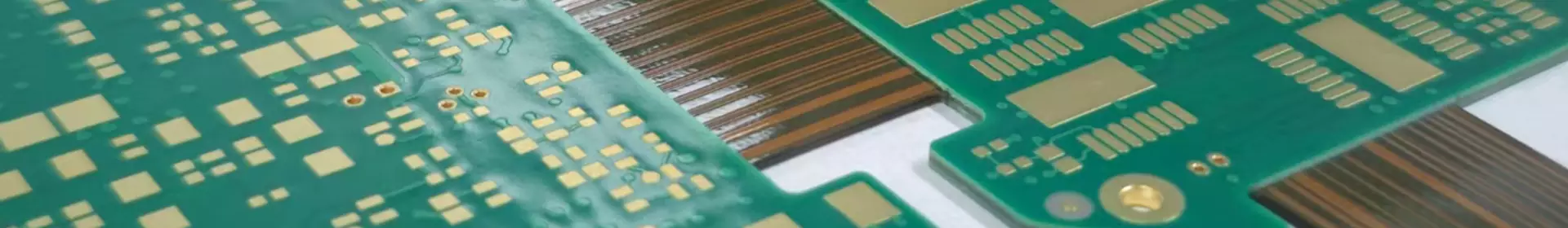
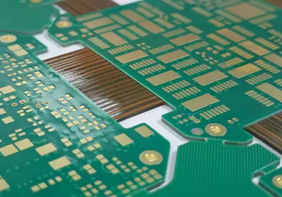
In PCB design, the solder mask plays a critical role, primarily preventing solder shorts during the soldering process, protecting circuits from environmental corrosion, and providing electrical insulation. The solder mask forms a protective layer on the physical board through negative film output, allowing copper traces to remain exposed in designated areas for soldering. During design, appropriate openings must be created in the solder mask, and pads must be extended outward to ensure soldering integrity. Additionally, the thickness and uniformity of the solder mask affect signal transmission quality. Therefore, its fabrication and design constitute a critical step in ensuring circuit performance and reliability during PCB development.

Four Primary Types of Solder Mask
Solder mask prevents conductive solder bridges between various electronic components. Essentially, it blocks short circuits. Different PCB solder mask types are as follows:
• Top and Bottom Masks: The electronics engineer knows the various openings. He understands what has been added via ink, epoxy, or film technology. Then, with the help of marked positions, he can solder component leads onto the board. One can also observe the pattern of conductive traces on the board's top surface. These are termed top traces. The lower surface is referred to as the bottom mask.
• Liquid Epoxy: For a cost-effective option, choose liquid epoxy. This thermosetting polymer has multiple applications. Screen printing is a printing technique that uses a woven mesh to support the solder resist pattern. The mesh creates an open area for ink transfer.
• Photoresist Liquid Ink: We offer solder mask as an ink formulation. The ink can be sprayed onto the PCB. Subsequently, the pattern can be exposed and developed. Note that this process, along with the liquid ink formulation, requires a clean environment free of contaminants and particles. After exposure to ultraviolet light, it can be removed using a high-pressure water spray known as a developer.
• Photoresist Dry Film Imaging: Apply this solder mask layer via vacuum lamination. After development, create openings and solder components to copper pads. Additionally, use solder to protect copper circuits. Then remove the dry film.
Why Apply Solder Mask to PCB Circuit Boards?
In printed circuit board (PCB) manufacturing, applying solder mask ink is a critical process. The primary functions of solder mask on PCB boards include: protecting circuits by preventing unintended solder adhesion to conductors, preventing electrical shorts between conductors caused by moisture or chemicals, preventing open circuits resulting from improper handling during subsequent production processes or electrical assembly, and shielding PCB boards from various harsh environmental conditions.
Both sides of a PCB are copper layers. Without a solder mask, exposed PCBs oxidize easily when exposed to air, becoming defective products and compromising electrical performance. Therefore, a protective coating must cover the PCB surface to prevent oxidation reactions with air. This coating is the solder mask layer applied using solder mask materials. Solder mask paints in various colors have emerged accordingly, resulting in colorful PCB circuit boards. However, the color of the solder mask has no bearing on the quality or electrical performance of the PCB board.
The PCB board surface also requires soldering electronic components, necessitating partial exposure of the copper layer for component attachment. This exposed copper area is known as the solder pad. As mentioned earlier, exposed copper layers are prone to oxidation. Therefore, pads also require a protective layer to prevent oxidation. This led to the development of pad plating, commonly referred to as PCB surface treatment. This can involve plating with inert metals like gold or silver, or applying special chemical films to prevent the copper layer of the pads from oxidizing when exposed to air.

The impact of the solder mask layer on PCBs is primarily reflected in the following aspects:
1. Dielectric Constant (Dk) and Loss Factor (Df)
The dielectric constant and loss factor (Df) of the solder mask affect signal transmission quality. A solder mask with a low dielectric constant and a low loss factor helps reduce signal attenuation and reflection. In high-frequency circuits, a higher dielectric constant (Dk) of the solder mask slows signal propagation speed, potentially causing signal delay. A higher loss factor (Df) in the solder mask results in greater energy loss during signal transmission and increased signal attenuation.
2. Signal Integrity
In high-frequency or high-speed signal transmission, the dielectric constant of the solder mask affects signal propagation speed. Mismatched dielectric constants between the solder mask and substrate material can cause signal reflection and distortion. The thickness and uniformity of the solder mask also impact impedance control precision, thereby affecting signal integrity.
3. Thermal Properties
Solder mask possesses thermal conductivity and a thermal expansion coefficient. If the solder mask's thermal expansion coefficient mismatches the substrate material, stresses generated during temperature changes can cause cracking or delamination of the solder mask, compromising the reliability of electrical connections.
4. Insulation Properties
The insulation properties of the solder mask directly affect PCB reliability. Poor solder mask quality, such as uneven thickness or defects, may cause insulation failure, leading to short circuits or leakage.
5. Soldering Quality
The solder mask defines soldering areas, preventing solder flow into unintended regions and ensuring soldering quality. Improper solder mask design—such as excessively large or small apertures, or using overly thick ink when defining pads—can cause soldering defects. Surface smoothness and adhesion of the solder mask also affect soldering quality, which in turn impacts electrical performance.
6. Environmental Protection
Poor solder mask quality or incomplete coverage allows moisture or contaminants from the environment to penetrate the PCB, leading to issues like reduced insulation resistance and increased leakage current. In high-humidity or corrosive environments, solder mask integrity is critical for long-term PCB reliability.

Summary
In summary, the solder mask plays a vital role in PCB design and manufacturing. It not only provides electrical insulation and circuit protection but also significantly contributes to the reliability and performance of electronic devices by enhancing aesthetics and improving soldering quality.