A Trustworthy PCB and Electronic Manufacturing Enterprise! Contact Us

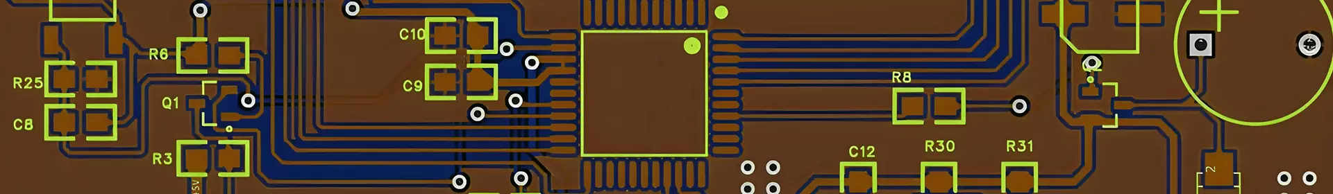
PCB Mark is a reference point used by machines to locate PCB boards during automated soldering. Typically, PCB boards with surface-mount components require mark points. During mass production, the pick-and-place machine can manually or automatically locate these mark points for calibration, providing a common reference for positioning circuit patterns throughout all assembly steps. Therefore, mark points are critical to SMT production.

Classification and Functions of PCB Mark
1. Global Mark Points (Board-Level Mark Points): Used for positioning individual circuit boards. Located at the edges or corners of the PCB, these points enable equipment such as pick-and-place machines to determine the board's overall position, orientation, and any potential warping. This ensures all components are accurately placed in their designated locations.
2. Local Markers: Used for components requiring precise positioning. Compared to global markers, local markers are typically positioned near specific components, particularly fine-pitch components (e.g., BGAs, CSPs, QFPs), which demand ultra-high placement accuracy. They provide more precise positional references for individual components, helping compensate for positioning inaccuracies caused by minor deviations during PCB manufacturing.
3. Panel Markers (Process Edge Markers): Used for positioning entire panel assemblies. They assist in locating all circuit features on the panel and facilitate positioning.
Four Key Elements of PCB Mark Design
1. Shape Specifications: Two common types: outer ring as a circle or hexagon, with a solid circular centre.
2. Composition Requirements: A complete marker includes: a solid circular “marker point” and a surrounding “clearance protection ring” free of traces and copper.
3. Size Constraints: Mark diameter: 1mm to 3mm; Clearance area: Minimum radius must exceed the mark radius; doubling the radius is recommended for improved recognition rates.
4. Edge Distance Specifications: Mark points must be ≥ 5mm from PCB edges to prevent obstruction by fixtures.

PCB Mark Recognition Mechanism
A mark point is typically an isolated copper pad distant from other visible landmarks, devoid of pads or circuit features. This ensures the machine vision system can clearly capture the point and use it as a reference to determine the positions of other components.
The mark recognition mechanism primarily relies on the vision system, as follows:
1. High Contrast: Mark points are generally designed with high-contrast features, typically white dots on a black background or vice versa. This enables the vision system to easily distinguish the Mark point from its surroundings.
2. Fixed Shape and Size: The shape and dimensions of Mark points are predefined and maintained consistently throughout production. This facilitates rapid and accurate recognition by the machine.
3. Fixed Position: Each Mark point occupies a fixed location relative to other features on the PCB (such as component placements). By identifying these points, the machine calculates the precise position and orientation of the entire PCB.
4. Image Processing Technology: Advanced image processing algorithms analyse camera-captured images of the mark points. These algorithms may include edge detection, morphological operations, template matching, and other methods to determine the exact centre position of the mark points.
5. Compensation Mechanism: Once mark points are identified, SMT (Surface Mount Technology) equipment can fine-tune component placement based on the actual detected positions, compensating for deviations caused by PCB manufacturing tolerances, thermal expansion, and other factors.
How to Design Mark Points?
1. Shape
While some manufacturing equipment is programmed to recognise various shapes like ovals, squares, or hourglasses, not all machines can handle them. Mark points are generally designed as solid circles because circular objects are easier for machines to locate. Additionally, the centre of a circle remains consistent regardless of viewing angle, enhancing positioning accuracy. Additionally, circles offer minimal surface area, uniform etching, and resistance to deformation. They also provide a stark contrast to traditional rectangular functional areas on circuit boards, facilitating machine recognition.
2. Dimensions
Marker point diameters typically range from 1.0mm to 3.0mm, depending on the assembly machinery used by the manufacturer. To ensure consistency, all marker points on a single board should be identical in size, with variations not exceeding approximately 25 microns. The minimum diameter of the resist layer (clear area) should be twice that of the exposed copper diameter of the mark point. This area must remain unobstructed, free from silkscreen or other elements. This ensures the machine vision system can clearly identify the mark points without interference.
3. Positioning
Mark points should be positioned at opposite diagonal corners of the circuit board, spaced as far apart as possible, ideally distributed along the longest diagonal. This layout helps minimise errors caused by PCB warping.
a. For PCBs shorter than 200mm, place at least 2 Mark points;
b. For PCBs longer than 200mm, place 4 Mark points; position 1 or 2 Mark points along or near the centerline of the PCB's long edge.
C. PCB Marker Points: Marker points should be placed along the diagonal of each sub-board.
4. Quantity
Generally, three reference points provide the optimal number for eliminating unexpected misalignment between the stencil and PCB.
Additionally, depending on the PCB's specific characteristics, multiple marker points may be required. For example: Single-sided assembly PCBs should have at least one pair of marker points positioned diagonally on each surface-mount side; For double-sided assembly, each side should have alignment marks. Furthermore, for complex components with fine pin pitches (such as QFP, CSP, BGA, etc.), additional local alignment marks are required to enhance placement accuracy.

Conclusion
PCB Mark is an indispensable part of modern electronics manufacturing, providing robust support for achieving high-precision and high-efficiency PCB production and assembly.