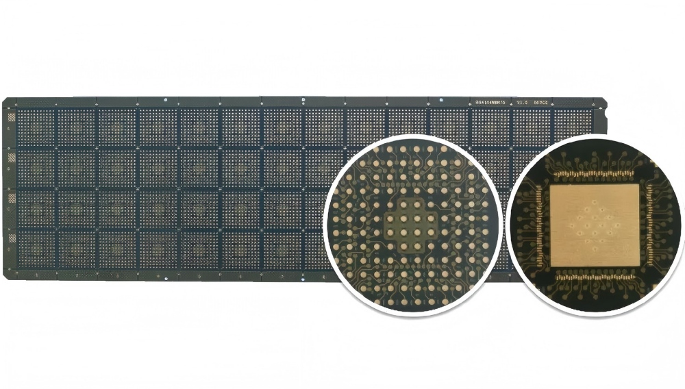
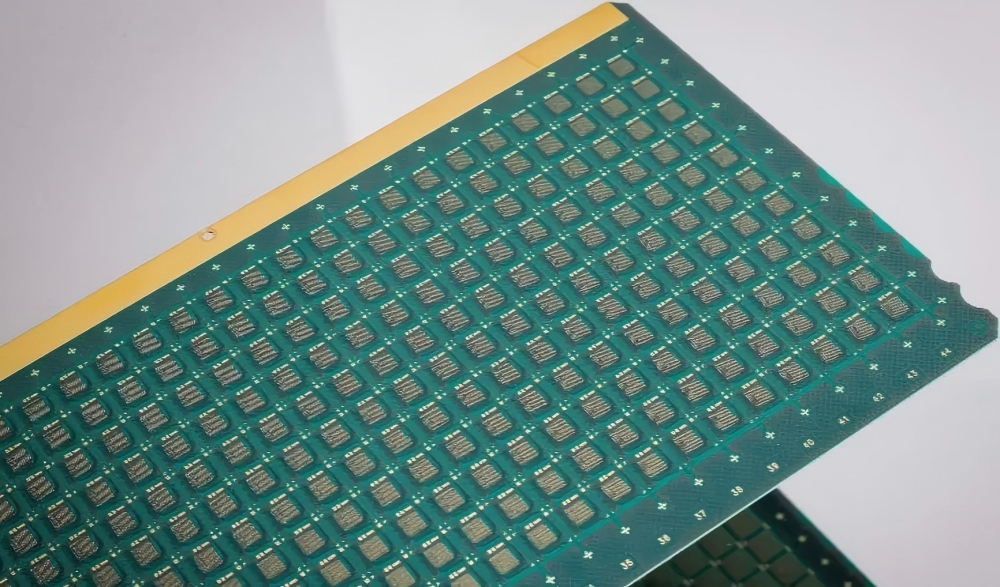
An IC substrate is a PCB used to package microchips. It can also be referred to as an IC carrier board. It connects the chip's minute connections to the larger structures of conventional circuit boards, such as motherboards. The substrate also supports and reinforces the IC, providing a mechanical foundation to prevent damage to the delicate circuits and components. Additionally, the substrate aids in heat dissipation, enabling the chip to operate cooler and more efficiently.

Key Properties and Characteristics of IC Substrate PCBs
IC substrate PCBs possess specific attributes distinct from standard PCBs. These characteristics are essential for ensuring IC substrate PCBs can support advanced ICs and meet the performance demands of modern electronics:
1. Compact Size: Typically small in dimension, designed to house a single chip or a few chips, which is critical for space-constrained devices.
2. Thin Profile: IC substrate PCBs range from 0.1 mm to 1.5 mm in thickness, offering a slim form factor suitable for compact electronics.
3. High-Density Interconnects: Featuring micro laser drilling and fine traces, IC substrate PCBs handle complex, high-density connections essential for integrating powerful chips.
4. Thermal Management: Substrates are engineered with heat-dissipating materials to ensure chips remain cool and perform optimally.
5. Electrical and Mechanical Support: Substrates guarantee efficient electrical signal transmission while providing the mechanical strength needed to protect ICs from physical damage.
6. Customizable: With advancements in manufacturing, IC substrate PCBs can be tailored to specific requirements—whether for high-performance, flexible, or miniature applications.
IC Substrate Classification:
1. By Packaging Type
a. BGA Package Substrates
Technical Advantages: Significantly increases chip pins while delivering excellent thermal dissipation and electrical performance.
Application Areas: Suitable for IC packages exceeding 300 pins.
b. CSP Package Substrates
Technical Advantages: Single-chip packaging, lightweight, and compact size.
Application Areas: Used in memory products, telecommunication products, and electronics with a small number of pins.
c. FC Package Substrates
Technical Advantages: Through flip-chip packaging, it offers low signal interference, low circuit loss, excellent performance, and effective heat dissipation.
Application Areas: Widely used in CPUs, GPUs, chipsets, and similar products.
d. MCM Packaging Substrates
Technical Advantages: Integrates chips with different functions into a single package. Features include lightweight, thin, short, and miniaturized characteristics. However, due to multiple chips within one package, this substrate type performs poorly in signal interference, heat dissipation, and fine routing.
Application Areas: Used in military and aerospace fields.
2. By Packaging Material
a. Rigid Substrates
Primary Materials & Applications: BT Resin (MEMS, communication and memory chips, LED chips), ABF Material (used in high-end chips like CPUs, GPUs, and chipsets), MIS (applied in analog, power ICs, and digital currency markets).
b. Flexible Substrates
Primary Materials and Applications: PI, PE (used in automotive electronics, consumer electronics, and military applications like launch vehicles, cruise missiles, and satellites).
c. Ceramic Substrates
Primary Materials and Applications: Aluminum Oxide, Aluminum Nitride, Silicon Carbide (used in semiconductor lighting, lasers and optical communications, aerospace, automotive electronics, deep-sea drilling, etc.).

3. By Application Field
a. Storage Chip Packaging Substrates (eMMC): Primarily used in storage modules for smartphones and tablets, solid-state drives, etc.
b. Micro-Electro-Mechanical Systems Packaging Substrates (MEMS): Primarily used in sensors for smartphones, tablets, wearable electronics, etc.
c. Radio Frequency Module Packaging Substrates (RF): Primarily used in RF modules for mobile communication products like smartphones.
d. Processor chip WB-CSP, primarily used for baseband and application processors in smartphones, tablets, etc.
e. Processor chip FC-CSP, primarily used for baseband and application processors in smartphones, tablets, etc.
f. High-speed communication packaging substrates, primarily used for conversion modules in data broadband, telecommunications, FTTX, data centers, security surveillance, and smart grids.
IC Substrate Manufacturing Challenges
1. Material Handling and Thickness Control
IC substrates are typically very thin, especially those under 0.2 mm thick. This makes them prone to warping during manufacturing. To overcome this challenge, manufacturers must employ advanced lamination techniques, precise layer alignment, and strictly control shrinkage and warpage throughout production.
2. Microvia and Fine-Line Technology
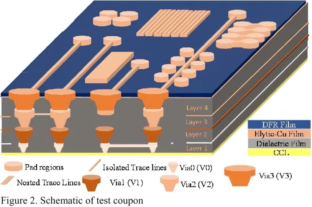
High-density interconnect requirements necessitate via technology, which involves laser drilling to connect different substrate layers. The challenge lies in ensuring uniform via diameter and defect-free copper filling. Additionally, fine line technology is critical for creating narrow conductive traces capable of supporting high-frequency signals.
3. Pattern Formation and Copper Plating
Copper plating and patterning are essential for defining circuit designs on the substrate. This requires precise control of plating thickness and the use of techniques like photolithography to ensure accurate, flawless formation of conductive traces.
4. Surface Finishing and Solder Mask Application
The surface finish of IC substrates is critical to their performance. Surfaces must be smooth and uniform to ensure reliable electrical connections and minimize oxidation risks. Solder mask application must also be precise to avoid defects that could compromise substrate performance.

Conclusion
IC substrate PCB boards serve as fundamental components in modern electronics, enabling the integration of advanced integrated circuits (ICs) into compact, high-performance devices. These carrier boards are critical across industries ranging from consumer electronics to aerospace, providing essential mechanical support, electrical routing, and thermal management functions. As demand for smaller, more efficient electronic products continues to grow, the role of high-quality PCB manufacturers becomes increasingly vital.